Research Article | | Peer-Reviewed

Ab-initio Study of the Optoelectronic Properties of a Semiconductor Under the Influence of an External Electric Field: The Case of Silicon (Si)

Received: 21 January 2026     Accepted: 3 February 2026     Published: 26 February 2026
Views:       Downloads:
Abstract

DFT calculations are performed on the structural, electronic, and optical properties of fcc silicon (Si). The plane wave (PW) method using Perdew-Burke-Ernzerhof generalized gradient approximation (PBE-GGA) exchange correlation potentials is applied to solve the Kohn-Sham equations. Energy convergence was examined to study ground-state properties. Band structure and total density of states (TDOS) diagrams are plotted from the calculated equilibrium lattice parameters. An electric field on the order of E=0 V/Å and E= 1V/Å is applied to the silicon surface. Band structure and energy density of Si at electric field E=0 V/A and E= 1V/A is studied in this paper. We also studied variation of the Fermi energy of Si as a function of the applied electric field. On simulate real part of the dielectric function ɛ1(ω) and Imaginary part of the dielectric function ɛ2(ω) as a function of the photon energy for Si with electric field E=0 V/Å and E= 1V/Å (10 GV/m). General profiles of the optical spectra under ambient conditions with and without an electric field are calculated. This study shows that applying an electric field normal to the surface of silicon modifies its electronic and optical properties. The band gap of silicon contracts, with the appearance of band degeneracy. The peak amplitude of its absorption coefficient, the dielectric function and the refractive index decrease in the ultraviolet range and increase in the visible range.

Published in American Journal of Physical Chemistry (Volume 15, Issue 1)
DOI 10.11648/j.ajpc.20261501.11
Page(s) 1-7
Creative Commons

This is an Open Access article, distributed under the terms of the Creative Commons Attribution 4.0 International License (http://creativecommons.org/licenses/by/4.0/), which permits unrestricted use, distribution and reproduction in any medium or format, provided the original work is properly cited.

Copyright

Copyright © The Author(s), 2026. Published by Science Publishing Group

Keywords

Silicium, Ab-initio, DFT Calculations, TDOS

1. Introduction
Optical properties play a crucial role in understanding the nature of materials and inform their use in optoelectronic devices. Applying a strong external electric field to the surface of a semiconductor is expected to induce significant changes in band structures and, consequently, in the material's optical properties .
Applying an intense electrostatic field to silicon can induce a modification of its band structure, a phenomenon often linked to the Stark effect or structural polarization in nanoscale devices (such as nanowires or ultrathin films) .
The resulting reduction in the band gap width offers several strategic advantages for electronic and optoelectronic components .
In this work, we consider the case of silicon subjected to fields of E=0 V/Å and E= 1V/Å. The objective is to study the electronic and optical properties and the energy modification of states at the silicon surface under these conditions, specifically the optical properties, the band gap, and the total density of states (TDOS), using ab initio calculations with the QANTUM ESPRESSO software. Fundamental principles calculations are used to study the influence of applying an electric field on the electronic structure and optical properties of silicon. In the case of an electric field (EZ) normal to the silicon crystal surface, a perturbation of the electron Hamiltonian by the electrostatic potential is expected. This leads to the modification of the system's Hamiltonian H according to the following equation:
H=H0+eEZ
Where H0 is the Hamiltonian of the system without an external electric field.
Our article can be summarized as follows: Section 2 presents the details of the calculations and a brief description of the calculation method. Section 3 presents the results of this calculation. Finally, the conclusions are presented in Section 4.
2. Methology
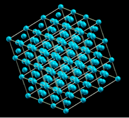
Figure 1. Structure of the silicon crystal lattice for 280 Si atoms.
We performed first-principles calculations based on density functional theory (DFT) to predict the electronic and optical properties of silicon Si. All DFT calculations reported in this manuscript are obtained using the Quantum ESPRESSO suite , with plane-wave expansion and norm-preserving relativistic scalar pseudopotentials . The electron exchange and correlation functionals were treated using the Perdew-Burke-Ernzerhof (PBE) generalized gradient approximation . The system under study is a fcc cube with periodic boundary conditions. After a convergence test, a plane-wave basis kinetic energy cutoff of 30 Ry, a 4×4×4 Monkhorst–Pack k-point uniform mesh , and the equilibrium lattice parameter a = 5.486 Å are used. We introduce an electric field in the (z) direction normal to the plane of the Si crystal and then discuss how the band structures change under the effect of this external electric field.
It is generally accepted that the interaction of a photon with the electrons of the system can be described by temporal perturbations of the ground electronic states. The transitions between occupied and unoccupied states are caused by the electric field of the photon. The spectra resulting from these excitations can be described as a joint density of states between the valence and conduction bands.
The optical response of a material to the electromagnetic field, at all energy levels, can be described by the complex dielectric function ε(ω) as follows:
εω=ε1ω+iε2ω
Where ε₁(ω) and ε₂(ω) are the real and imaginary parts of the dielectric function. The real part of the dielectric function represents the scattering of incident photons by the material, while the imaginary part of the dielectric function corresponds to the energy absorbed by the material. The calculation of these components of the dielectric function is associated with the energy eigenvalue and the energy wave functions, which are the direct output of the band structure calculation. From knowledge of ε₁(ω) and ε₂(ω), all other optical properties, such as reflectivity R(ω), refractive index n(ω), extinction coefficient κ(ω), energy loss function L(ω), absorption coefficient α(ω), and optical conductivity σ(ω), can be calculated .
Rω=n-12+k2n+12+k2
Where n and k are respectively the real and imaginary parts of the complex refractive index.
nω=ε12ω+ε22ω+ε1ω2
kω=ε12ω+ε22ω-ε1ω2
Lω=ε2ωε12ω+ε22ω
αω=ω2ε12ω+ε22ω-ε1ω
Rσω=ω4πε2ω
3. Results and Discussion
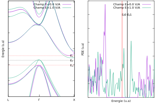
Figure 2. Band structure and energy density of Si at electric field E=0 V/A and E= 1V/A.
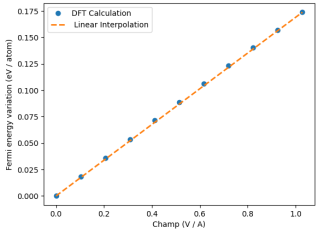
Figure 3. Variation of the Fermi energy of Si as a function of the applied electric field. The Fermi level follows the following relationship: Ef = Ef0 + 0.169EZ, where EZ is the electric field strength and Ef0 is the Fermi energy with zero electric field.
The electronic properties of Si are studied using the band structure and the total density of states (TDOS) calculated with optimized values . Spin-unpolarized calculations are performed . The calculations are carried out along the L-Γ-X top symmetry points in the Brillouin zone. Our results in Figure 2 show a contraction of the band gap between the valence and conduction band states, leading to a significant curvature of the band structure at a strong electric field of 1 V/Å. We also observe the emergence of new energy states (degeneracy) and the Fermi level shift under the effect of this applied electric field . Figure 3 shows that this Fermi level shift follows a linear law with the amplitude of the electric field. This is due to the electric polarizability, which is proportional to the EZ field. The maximum of the valence band EV and the minimum of the conduction band EC are located at points G and X, respectively, resulting in an indirect band gap. EV = 5.9638 and EC = 6.5703 without a field, and EV = 6.3025 and EC = 6.4249 at EZ = 1 V/Å. Therefore, the band gap of undoped Si is Eg = 0.6056 eV without an electric field. This band gap value, lower than the experimental value of 1.12 eV for pure Si, is expected because the DFT calculation with Quantum Espresso systematically underestimates energy gaps. When the electric field increases from 0 to 1 V/Å, the band gap decreases from 0.6056 eV to 0.1224 eV, a reduction of x = 79.79%. Therefore, the predicted experimental value of the band gap is 1.12(1-x/100), or 0.2223 eV under an EZ field of 1 V/A. The band gap response of silicon under the influence of an electric field modifies the electronic properties of silicon. We observe that the inclusion of EZ changes the energy level of silicon. Consequently, under the effect of EZ on the order of a few tenths of a V/μ, the band gap still indicates the semiconducting properties of silicon. Thus, the band gap can be significantly controlled by the influence of EZ.
Figure 2b illustrates the total density of states of silicon as a function of EZ. The description of these states defines the conductive properties of silicon. The state of all atoms in the silicon crystal structure near the Fermi level is primarily derived from the 3pz orbital of silicon 3p. Due to the decrease in band gap energy, the probability of occupation of electrons near the Fermi level increases.
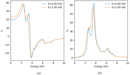
Figure 4. (a) Real part of the dielectric function ɛ1(ω) and (b) Imaginary part of the dielectric function ɛ2(ω) as a function of the photon energy for Si with electric field E=0 V/Å and E= 1V/Å i.e. 10 GV/m.
Figure 4 shows the complex dielectric function ε(ω) as a function of frequency in the range of 0 to 10 eV. It describes the optical properties of silicon interacting with light. Its real part, ε₁(ω), determines the dispersion effects, and its imaginary part, ε₂(ω), determines the absorption effects.
It can be observed that under the effect of EZ, the peaks of ε₁(ω) and ε₂(ω) increase in the visible region while they decrease in the UV region. These results demonstrate the ability of silicon to absorb photons in the visible range when EZ is applied in the Z direction normal to the crystal surface. The ε₂(ω) portion exhibits two prominent peaks in the range of 2 to 10 eV, related to interband transitions. The maximum peak is recorded for an incident photon energy of 3.79 eV, where absorption is maximal. It is important to note that for values of ε2(ω) = 0, at low energy and towards the end of the UV there is no absorption, because electrons cannot react at EZ. The value of the static dielectric constant (the value of the dielectric constant at zero energy) ε1(0) is 19.4475 without an electric field and 22.2660 at EZ = 1 V/Å.
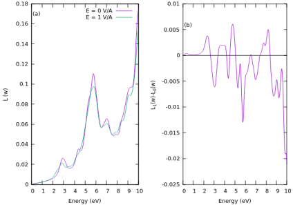
Figure 5. Energy loss function L(ω) as a function of photon energy for Si with electric field E=0 V/Å and E= 1V/Å.
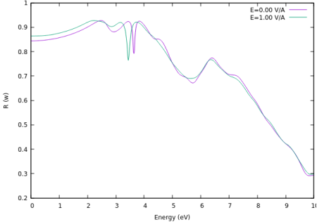
Figure 6. Reflectivity spectra R(ω) as a function of photon energy for Si at electric field E=0 V/Å and E= 1V/Å.
Figures 5 and 6 show the reflectivity and energy loss spectra of silicon. Reflectivity is significant at low photon energies. The reflectivity of pure silicon as a function of the applied electric field is illustrated in Figure 6. It can be seen that the reflectivity is higher at low energies, therefore the transition probability is lower at low energies. The static refractive index (the refractive index value at zero energy) is 4.40208 without an external electric field, while it is 4.7330 when an electric field is applied, as shown in Figure 7a.
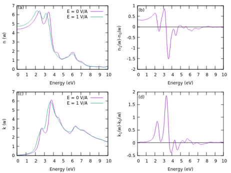
Figure 7. (a), (b) real part of the refractive index and (c), (d) Imaginary part of the refractive index as a function of the photon energy for Si, at electric field E=0 V/Å and E= 1V/Å.
Figure 6 illustrates the complex refractive index n*(ω) = n(ω) + ik(ω) of Si, which describes the propagation of light in this absorbing material. The imaginary part k(ω) deals with attenuation, while the real part n(ω) deals with refraction . The above values of the static dielectric constant ε1(0) and the static refractive index n(0) satisfy the relation n = √ε1 (Table 1). When EZ is applied to the surface of Si, the part n(ω) varies with frequency. Therefore, Si is a dispersive material, and its dispersion is affected by EZ. The refractive index increases in the visible and decreases in the ultra violet (UV), because the application of EZ causes collisions and interactions between incident photons and electrons within Si. Furthermore, the component k(ω) increases in the visible. Analysis of the graphs of ε2(ω) and k(ω) shows similar physical behavior in Figures 5 and 6. These two physical quantities provide information on the absorption of light by the Si crystal structure. Without an external EZ field, the absorption spectrum consists of three peaks of different intensities. The intensity of the first peak is 2.71 eV, that of the second is 3.79 eV, and that of the third is 6.44 eV . The first two peaks originate from two fundamental (interband) transitions between the electronic states of Si. The first peak corresponds to the transition from the occupied to the unoccupied state in the conduction band. The second peak corresponds to the Si-Si transition from the π-π* state near the Fermi level in the sp3 hybrid region . The third peak originates from the intraband transition. Based on these three peaks, the Si crystal exhibits strong light absorption, capable of absorbing in the visible and UV ranges. In the visible range, the intensity of the absorption peak increases when a voltage EZ = 1 V/Å is applied in the z-direction normal to the Si crystal, due to the decrease in the band gap energy. When EZ is applied, it causes a shift of the absorption peak towards the infrared (IR) range, due to the decrease in the band gap energy . This behavior suggests that EZ can be used effectively to tune the absorption of Si. Furthermore, its application to Si increases its light absorption capacity in the visible range. According to our absorption spectrum calculation results, silicon possesses optical properties dependent on the effect of EZ.
Table 1. The static dielectric constant ε1(0) and the static refractive index n(0) of Si under an external electric field EZ.

E (V/Å)

0

1

n(0)

4.40208

4.7330

ɛ1(0)

19.4475

22.2660

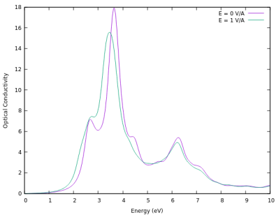
Figure 8. Optical conductivity σ(ω) as a function of photon energy for Si at electric field E=0 V/A and E= 1V/A.
4. Conclusion
This ab initio study quantified the impact of an external electric field (Ez=1 V/Å) on the properties of silicon.
Applying the field induces a strong perturbation of the Hamiltonian, resulting in an 80% band gap contraction (from 0.61 to 1.12 eV) and the lifting of band degeneracy. The Fermi level exhibits a linear shift proportional to the field intensity.
The band gap reduction promotes increased absorption in the visible range, while a decrease is observed in the ultraviolet. This intensity shift towards lower energies (redshift) is confirmed by the evolution of the imaginary parts of the dielectric function ε²(ω) and the refractive index k(ω).
By validating the relation n≈√(ε₁) under a strong electric field, we demonstrated the consistency of our calculations.
In summary, these results demonstrate that silicon, under the influence of an intense electric field, becomes an optically tunable material. This property paves the way for the design of electro-optical modulators and controlled absorption photovoltaic devices.
Abbreviations

PWX

Plane Wave

PBE

Generalized Gradient Approximation

GGA

Perdew-Burke-Ernzerhof

TDOS

Total Tensity of States

DFT

Density Functional Theory

Conflicts of Interest
The authors declare no conflicts of interest.
References
[1] C. Kittel and S. Johnson, Introduction to Solid State Physics, EIGHTH edi. Berkeley, 2005.
[2] M. Kria et al., “Quantum Confined Stark Effect on the Linear and Nonlinear Optical Properties of SiGe / Si Semi Oblate and Prolate Quantum Dots Grown in Si Wetting Layer,” 2021.
[3] J. S. De Sousa and V. N. Freire, “Intraband absorption and Stark effect in silicon nanocrystals,” pp. 1–8, 2005,
[4] H. Mathieu and H. Fanet, Physique des semiconducteurs et des composants electroniques: Cours et exercices corriges, Dunod. Paris, 2009. [Book on semiconductors (course and solved exercises)]. Available:
[5] Y. Choi et al., “Ultrathin-Body SOI MOSFET for Deep-Sub-Tenth,” vol. 21, no. 5, pp. 254–255, 2000.
[6] M. S. L. Yang Liu, Gerhard Klmeck, Neophytos Neophytou, “Band-Structure Effects on the Band-Structure Effects on the Performance of SoI MOSFETs,” IEEE Trans. Electron Devices, vol. 55, no. 05, pp. 1116–1122, 2008.
[7] P. Giannozzi et al., “QUANTUM ESPRESSO: A modular and open-source software project for quantum simulations of materials,” J. Phys. Condens. Matter, vol. 21, no. 39, 2009,
[8] P. Giannozzi et al., “Quantum ESPRESSO toward the exascale,” J. Chem. Phys., vol. 152, no. 15, 2020,
[9] A. Gaur, K. Khan, A. Soni, A. Dashora, J. Sahariya, and U. Ahuja, “Theoretical analysis of Sn-doped ZnS for optoelectronic applications,” J. Phys. Conf. Ser., vol. 1504, no. 1, 2020,
[10] M. Fuchs and M. Scheffler, “Ab initio pseudopotentials for electronic structure calculations of poly-atomic systems using density-functional theory,” Comput. Phys. Commun., vol. 119, no. 1, pp. 67–98, 1999,
[11] S. M. Thompson et al., “Red Emission from Copper-Vacancy Color Centers in Zinc Sulfide Colloidal Nanocrystals,” ACS Nano, vol. 17, no. 6, pp. 5963–5973, 2023,
[12] C. C. Andrea Benassi, Andrea Ferretti, “P W SCF ’ s epsilon. x user ’ s manual,” Nanostructure and Biosystem at Surfaces, vol. 3, pp. 1–4.
[13] James R. Chelikowsky, “Nonlocal pseudopotential calculations for the electronic structure of eleven diamond and zinc-blende semiconductors* James,” Phys. Rev, vol. 14, no. 2, 1976.
[14] B. Shi et al., “Applied Surface Science Electric field effect of sliding graphene / hexagonal boron nitride heterobilayer,” Appl. Surf. Sci., vol. 636, no. May, p. 157816, 2023,
[15] Martin A Green, “Self-consistent optical parameters of intrinsic silicon at 300 K including temperature coefficients,” Sol. Energy Mater. Sol. Cells, vol. 92, pp. 1305–1310, 2008,
[16] D. E. A. and A. A. Studna, “Dielectric functions and optical parameters of Si, Ge, GaP, GaAs, GaSb, InP, InAs and InSb from 1.5 to 6.0 eV,” Phys. Rev, vol. 27, no. Number 2, 1983.
[17] M. L. Cohen and J. R. Chelikowsky, Electronic Structure and Optical Properties of Semiconductors, Springer. New York: Springer New York LLC.
Cite This Article
  • APA Style

    Alio, I. A., Hassan, A. A., Almoustapha, A. (2026). Ab-initio Study of the Optoelectronic Properties of a Semiconductor Under the Influence of an External Electric Field: The Case of Silicon (Si). American Journal of Physical Chemistry, 15(1), 1-7. https://doi.org/10.11648/j.ajpc.20261501.11

    Copy | Download

    ACS Style

    Alio, I. A.; Hassan, A. A.; Almoustapha, A. Ab-initio Study of the Optoelectronic Properties of a Semiconductor Under the Influence of an External Electric Field: The Case of Silicon (Si). Am. J. Phys. Chem. 2026, 15(1), 1-7. doi: 10.11648/j.ajpc.20261501.11

    Copy | Download

    AMA Style

    Alio IA, Hassan AA, Almoustapha A. Ab-initio Study of the Optoelectronic Properties of a Semiconductor Under the Influence of an External Electric Field: The Case of Silicon (Si). Am J Phys Chem. 2026;15(1):1-7. doi: 10.11648/j.ajpc.20261501.11

    Copy | Download

  • @article{10.11648/j.ajpc.20261501.11,
      author = {Issoufou Arzika Alio and Amadou Arifa Hassan and Aboubacar Almoustapha},
      title = {Ab-initio Study of the Optoelectronic Properties of a Semiconductor Under the Influence of an External Electric Field: The Case of Silicon (Si)},
      journal = {American Journal of Physical Chemistry},
      volume = {15},
      number = {1},
      pages = {1-7},
      doi = {10.11648/j.ajpc.20261501.11},
      url = {https://doi.org/10.11648/j.ajpc.20261501.11},
      eprint = {https://article.sciencepublishinggroup.com/pdf/10.11648.j.ajpc.20261501.11},
      abstract = {DFT calculations are performed on the structural, electronic, and optical properties of fcc silicon (Si). The plane wave (PW) method using Perdew-Burke-Ernzerhof generalized gradient approximation (PBE-GGA) exchange correlation potentials is applied to solve the Kohn-Sham equations. Energy convergence was examined to study ground-state properties. Band structure and total density of states (TDOS) diagrams are plotted from the calculated equilibrium lattice parameters. An electric field on the order of E=0 V/Å and E= 1V/Å is applied to the silicon surface. Band structure and energy density of Si at electric field E=0 V/A and E= 1V/A is studied in this paper. We also studied variation of the Fermi energy of Si as a function of the applied electric field. On simulate real part of the dielectric function ɛ1(ω) and Imaginary part of the dielectric function ɛ2(ω) as a function of the photon energy for Si with electric field E=0 V/Å and E= 1V/Å (10 GV/m). General profiles of the optical spectra under ambient conditions with and without an electric field are calculated. This study shows that applying an electric field normal to the surface of silicon modifies its electronic and optical properties. The band gap of silicon contracts, with the appearance of band degeneracy. The peak amplitude of its absorption coefficient, the dielectric function and the refractive index decrease in the ultraviolet range and increase in the visible range.},
     year = {2026}
    }
    

    Copy | Download

  • TY  - JOUR
    T1  - Ab-initio Study of the Optoelectronic Properties of a Semiconductor Under the Influence of an External Electric Field: The Case of Silicon (Si)
    AU  - Issoufou Arzika Alio
    AU  - Amadou Arifa Hassan
    AU  - Aboubacar Almoustapha
    Y1  - 2026/02/26
    PY  - 2026
    N1  - https://doi.org/10.11648/j.ajpc.20261501.11
    DO  - 10.11648/j.ajpc.20261501.11
    T2  - American Journal of Physical Chemistry
    JF  - American Journal of Physical Chemistry
    JO  - American Journal of Physical Chemistry
    SP  - 1
    EP  - 7
    PB  - Science Publishing Group
    SN  - 2327-2449
    UR  - https://doi.org/10.11648/j.ajpc.20261501.11
    AB  - DFT calculations are performed on the structural, electronic, and optical properties of fcc silicon (Si). The plane wave (PW) method using Perdew-Burke-Ernzerhof generalized gradient approximation (PBE-GGA) exchange correlation potentials is applied to solve the Kohn-Sham equations. Energy convergence was examined to study ground-state properties. Band structure and total density of states (TDOS) diagrams are plotted from the calculated equilibrium lattice parameters. An electric field on the order of E=0 V/Å and E= 1V/Å is applied to the silicon surface. Band structure and energy density of Si at electric field E=0 V/A and E= 1V/A is studied in this paper. We also studied variation of the Fermi energy of Si as a function of the applied electric field. On simulate real part of the dielectric function ɛ1(ω) and Imaginary part of the dielectric function ɛ2(ω) as a function of the photon energy for Si with electric field E=0 V/Å and E= 1V/Å (10 GV/m). General profiles of the optical spectra under ambient conditions with and without an electric field are calculated. This study shows that applying an electric field normal to the surface of silicon modifies its electronic and optical properties. The band gap of silicon contracts, with the appearance of band degeneracy. The peak amplitude of its absorption coefficient, the dielectric function and the refractive index decrease in the ultraviolet range and increase in the visible range.
    VL  - 15
    IS  - 1
    ER  - 

    Copy | Download

Author Information